Albis Optoelectronics is dedicated to supply products and services of outstanding quality. Our world-class on-site wafer manufacturing facilities offer full in-house production from front-end to back-end and includes a 2’000 sq ft class 100 cleanroom, assembly and packaging capabilities and extensive test and qualification laboratories.
Our custom fab services include full custom wafer processing, cleanroom processes, assembly and packaging services as well as device testing and characterization:
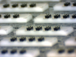
Custom Wafer Processing |
|
|
|
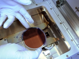
Cleanroom Services |
|

|
|
Dicing and Sawing |
|
|
|
Assembly and Packaging |
|

|
|
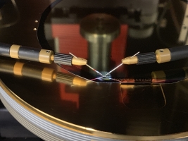
Electro-optical Device Characterization |
|
|
|
Mechanical Device Testing |
|

|
|
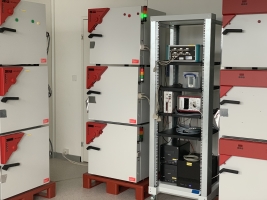
Environmental Device Testing |
|
|